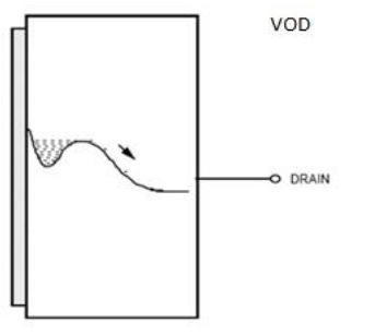
Blooming, or charge overflow into neighbouring pixels, is the result of electron overexposure when the pixel's full well capacity is exceeded. Overflow is most easily caused in the direction of the parallel register (in the direction of the column). To prevent blooming, so-called Overflow Drain (OD) channels can be used, into which electrons overflow earlier than into adjacent pixels (due to smaller barriers between pixel potential wells and drain channels than between two pixels). This is called anti-blooming.
Drain channels can be constructed in two ways:
- VOD = Vertical Overflow Drain - excess charge is drained to the depth of the substrate with an applied bias.
- LOD = Lateral Overflow Drain - the drain is located next to the pixel column, reducing the active area of the chip<
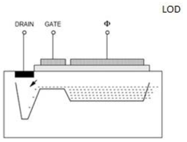
Drain channels can also serve as an electronic shutter - if the barrier to the channel is turned off, all generated charge drains away immediately. The disadvantages are degraded linearity and reduced pixel capacity.